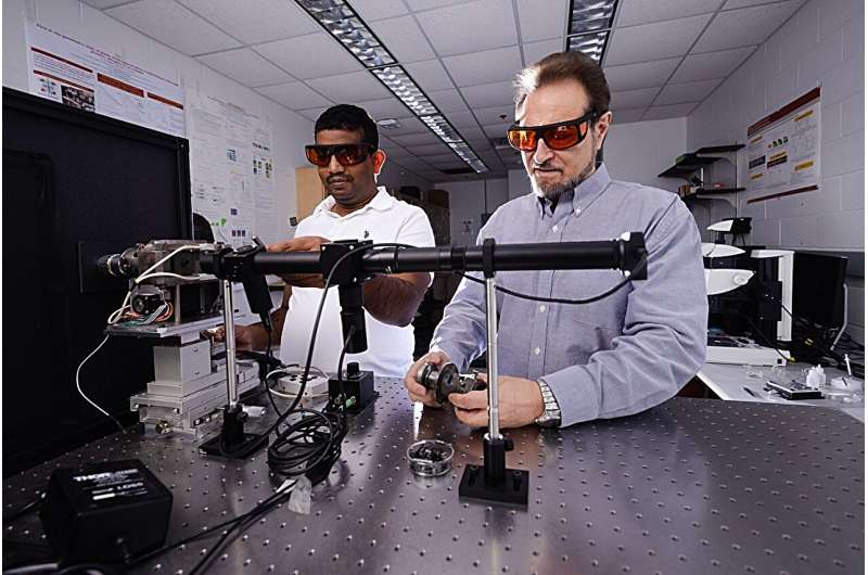
When Valery Levitas left Europe in 1999, he packed up a rotational diamond anvil cell and brought it to the United States. He and the researchers in his group are still using a much-advanced version of that pressing, twisting tool to squeeze and shear materials between two diamonds to see in situ, within the actual experiment, what happens and verify the researchers’ own theoretical predictions.
How, for example, do crystal structures change? Does that produce new, and potentially useful properties? Does the shearing change how high pressure needs to be applied to create new material phases?
It’s research “at the intersection of advanced mechanics, physics, material science, and applied mathematics,” wrote Levitas, an Iowa State University Anson Marston Distinguished Professor of Engineering and the Murray Harpole Chair in Engineering.
One of the latest findings from Levitas and his collaborators is that silicon, an important material for electronics, has unusual phase transformations when it is pressed and sheared with large and plastic, or permanent, deformations.
The journal Nature Communications recently published the findings. The corresponding authors are Levitas; and Sorb Yesudhas, an Iowa State postdoctoral research associate in aerospace engineering and the key experimentalist. Co-authors are Feng Lin, formerly of Iowa State; K.K. Pandey, formerly of Iowa State now at the Bhabha Atomic Research Centre in India; and Jesse Smith, of the High-Pressure Collaborative Access Team at Argonne National Laboratory in Illinois, where the group did in situ, X-ray diffraction experiments.
The researchers acknowledge there have been many studies of silicon’s changes under high pressure, but not of silicon under pressure and plastic shear deformation. In this case, they subjected three particle sizes of silicon—1 millionth of a meter, 30 billionths of a meter and 100 billionths of a meter—to the unique strains of the rotational diamond anvil cell.
Such “plastic strain-induced phase transformations are entirely different and promise numerous discoveries,” the researchers wrote.
One room-temperature experiment on silicon samples 100 billionths of a meter across found that pressures of 0.3 gigapascals, a common unit to measure pressure, and plastic deformations transformed silicon’s so-called “Si-I” crystal phase to “Si-II.” Under high pressure alone, that transformation starts at 16.2 gigapascals.
“Pressure is reduced by a factor of 54,” the authors wrote.
That’s a breakthrough experimental finding, Levitas said.
“One of our goals is to reduce transformation pressures,” he said. “So, we work in a region other researchers usually ignore—very low pressures.”
In addition, he said, the point of the researchers’ material deformations isn’t to change the shape or size of material samples.
“The key part is changing the microstructure,” Levitas said. “That makes the changes that produce phase transformations.”
And the different crystal lattice structures of the different phases—this paper considers seven phases of silicon—offers different properties that could be useful in real-world, industrial applications.
“Retrieving the desired nanostructured pure phases or mixture of phases (nanocomposites) with optimal electronic, optical and mechanical properties is possible with this technique,” the researchers wrote.
It’s a technique that industry could find interesting.
“Working with very high pressures for these phase transformations isn’t practical for industry,” Levitas said. “But with plastic deformations, we can get to these traditionally high-pressure phases, properties and applications at very modest pressures.”
After 20 years of thinking and theorizing about these material questions, Levitas said he expected silicon’s unusual response to the strains in the rotational diamond anvil cell.
“If I didn’t expect phase transformations at low pressures, we would have never checked,” he said. “These experiments confirm our several theoretical predictions and also open new challenges for the theory.”
